- 您现在的位置:买卖IC网 > Sheet目录17381 > ADP1829-EVALZ (Analog Devices Inc)BOARD EVALUATION ADP1829
�� �
�
�ADP1829�
�Data� Sheet�
�The� rest� of� the� system� gain� is� needed� to� reach� 0� dB� at� crossover.�
�The� total� gain� of� the� system,� therefore,� is� given� by�
�GAIN�
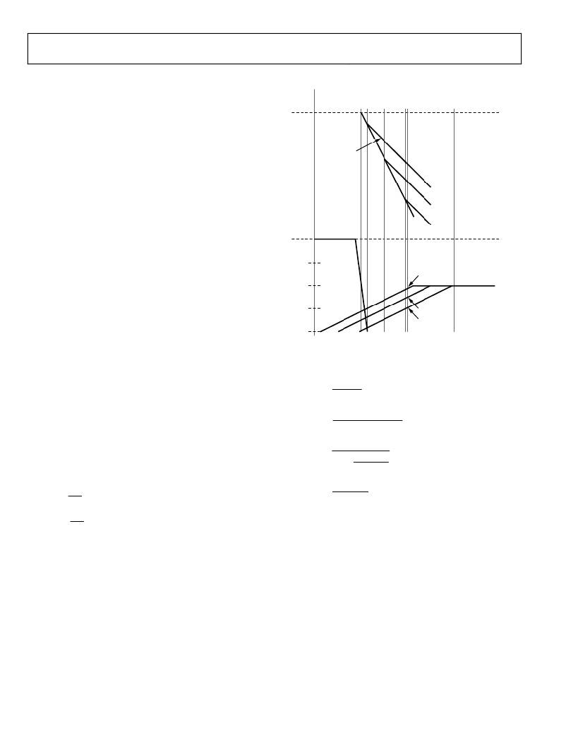
�LC� FILTER� BODE� PLOT�
�PHASE� CONTRIBUTION� AT� CROSSOVER�
�OF� VARIOUS� ESR� ZERO� CORNERS�
�A� T� =� A� MOD� +� A� FILTER� +� A� COMP�
�where:�
�(26)�
�0dB�
�f� LC� f� ESR1� f� ESR2� f� ESR3� f� CO�
�–40dB/dec�
�f� SW�
�FREQUENCY�
�A� MOD� is� the� gain� of� the� PWM� modulator.�
�A� FILTER� is� the� gain� of� the� LC� filter� including� the� effects� of�
�the� ESR� zero.�
�A� COMP� is� the� gain� of� the� compensated� error� amplifier.�
�Additionally,� the� phase� of� the� system� must� be� brought� back� up�
�to� guarantee� stability.� Note� from� the� bode� plot� of� the� filter� that�
�the� LC� contributes� ?180°� of� phase� shift.� Additionally,� because�
�the� error� amplifier� is� an� integrator� at� low� frequency,� it� contrib-�
�utes� an� initial� ?90°.� Therefore,� before� adding� compensation� or�
�accounting� for� the� ESR� zero,� the� system� is� already� down� ?270°.�
�To� avoid� loop� inversion� at� crossover,� or� ?180°� phase� shift,� a�
�good� initial� practical� design� is� to� require� a� phase� margin� of� 60°,�
�PHASE�
�0°�
�–20dB/dec�
�which� is� therefore� an� overall� phase� loss� of� ?120°� from� the� initial�
�low� frequency� dc� phase.� The� goal� of� the� compensation� is� to�
�boost� the� phase� back� up� from� ?270°� to� ?120°� at� crossover.�
�The� two� common� compensation� schemes� used� are� sometimes�
�referred� to� as� Type� II� or� Type� III� compensation,� depending� on�
�whether� the� compensation� design� includes� two� or� three� poles.�
�–90°�
�–180°�
�Φ� 1�
�Φ� 2�
�Φ� 3�
�(Dominant-pole� compensations,� or� single-pole� compensation,�
�is� referred� to� as� Type� I� compensation,� but� unfortunately,� it� is� not�
�very� useful� for� dealing� successfully� with� switching� regulators.)�
�Figure� 27.� LC� Filter� Bode� Plot�
�The� following� equations� were� used� for� the� calculation� of� the�
��2� ?� R� Z�
�If� the� zero� produced� by� the� ESR� of� the� output� capacitor� provides�
�sufficient� phase� boost� at� crossover,� Type� II� compensation� is�
�adequate.� If� the� phase� boost� produced� by� the� ESR� of� the� output�
�capacitor� is� not� sufficient,� another� zero� is� added� to� the�
�compensation� network,� and� thus,� Type� III� is� used.�
�In� Figure� 27,� the� location� of� the� ESR� zero� corner� frequency�
�gives� significantly� different� net� phase� at� the� crossover� frequency.�
�Use� the� following� guidelines� for� selecting� between� Type� II� and�
�Type� III� compensators:�
�f� Z1� ?�
�f� Z2� ?�
�f� P1� ?�
�1�
�2� ?� R� Z� C� I�
�1�
�2� ?� C� FF� (� R� TOP� ?� R� FF� )�
�1�
�C� I� C� HF�
�C� I� ?� C� HF�
�(27)�
�(28)�
�(29)�
�If� f� ESRZ� ?�
�f� CO�
�2�
�,� use� Type� II� compensation.�
�f� P2� ?�
�1�
�2� ?� R� FF� C� FF�
�(30)�
�If� f� ESRZ� ?�
�f� CO�
�2�
�,� use� Type� III� compensation.�
�where:�
�f� Z1� is� the� zero� produced� in� the� Type� II� compensation.�
�f� Z2� is� the� zero� produced� in� the� Type� III� compensation.�
�f� P1� is� the� pole� produced� in� the� Type� II� compensation.�
�f� P2� in� the� pole� produced� in� the� Type� III� compensation.�
�Rev.� C� |� Page� 20� of� 28�
�发布紧急采购,3分钟左右您将得到回复。
相关PDF资料
R1S-1515/P-R
CONV DC/DC 1W 15VIN 15VOUT
ADP2102-1.8-EVALZ
BOARD EVAL FOR ADP2102-1.8
ECM10DCMD-S288
CONN EDGECARD 20POS .156 EXTEND
ADP2102-1.875EVALZ
BOARD EVAL FOR ADP2102-1.875
195D685X0016X2T
CAP TANT 6.8UF 16V 20% 2910
A9BAG-1108F
FLEX CABLE - AFF11G/AF11/AFE11T
GEM12DSES-S243
CONN EDGECARD 24POS .156 EYELET
EBM08DCCN-S189
CONN EDGECARD 16POS R/A .156 SLD
相关代理商/技术参数
ADP1850
制造商:AD 制造商全称:Analog Devices 功能描述:Wide Range Input, Dual/Two-Phase, DC-to-DC Synchronous Buck Controller
ADP1850ACPZ
制造商:Analog Devices 功能描述:IC BUCK CNTRL SYNC 2PH 32LFCSP
ADP1850ACPZ-R7
功能描述:IC REG CTRLR BUCK PWM CM 32LFCSP RoHS:是 类别:集成电路 (IC) >> PMIC - 稳压器 - DC DC 切换控制器 系列:- 特色产品:LM3753/54 Scalable 2-Phase Synchronous Buck Controllers 标准包装:1 系列:PowerWise® PWM 型:电压模式 输出数:1 频率 - 最大:1MHz 占空比:81% 电源电压:4.5 V ~ 18 V 降压:是 升压:无 回扫:无 反相:无 倍增器:无 除法器:无 Cuk:无 隔离:无 工作温度:-5°C ~ 125°C 封装/外壳:32-WFQFN 裸露焊盘 包装:Digi-Reel® 产品目录页面:1303 (CN2011-ZH PDF) 其它名称:LM3754SQDKR
ADP1850DP-EVALZ
功能描述:EVAL BOARD FOR ADP1850DP RoHS:是 类别:编程器,开发系统 >> 评估板 - DC/DC 与 AC/DC(离线)SMPS 系列:- 标准包装:1 系列:- 主要目的:DC/DC,步降 输出及类型:1,非隔离 功率 - 输出:- 输出电压:3.3V 电流 - 输出:3A 输入电压:4.5 V ~ 28 V 稳压器拓扑结构:降压 频率 - 开关:250kHz 板类型:完全填充 已供物品:板 已用 IC / 零件:L7981 其它名称:497-12113STEVAL-ISA094V1-ND
ADP1850SP-EVALZ
功能描述:EVAL BOARD FOR ADP1850SP RoHS:是 类别:编程器,开发系统 >> 评估板 - DC/DC 与 AC/DC(离线)SMPS 系列:- 产品培训模块:Obsolescence Mitigation Program 标准包装:1 系列:True Shutdown™ 主要目的:DC/DC,步升 输出及类型:1,非隔离 功率 - 输出:- 输出电压:- 电流 - 输出:1A 输入电压:2.5 V ~ 5.5 V 稳压器拓扑结构:升压 频率 - 开关:3MHz 板类型:完全填充 已供物品:板 已用 IC / 零件:MAX8969
ADP1851ACPZ-R7
功能描述:电流型 PWM 控制器 w-range input Synch StepDown DC/DC Cntr RoHS:否 制造商:Texas Instruments 开关频率:27 KHz 上升时间: 下降时间: 工作电源电压:6 V to 15 V 工作电源电流:1.5 mA 输出端数量:1 最大工作温度:+ 105 C 安装风格:SMD/SMT 封装 / 箱体:TSSOP-14
ADP1851-EVALZ
功能描述:电源管理IC开发工具 Evaluation Board 1.8V 25A Output RoHS:否 制造商:Maxim Integrated 产品:Evaluation Kits 类型:Battery Management 工具用于评估:MAX17710GB 输入电压: 输出电压:1.8 V
ADP1853
制造商:AD 制造商全称:Analog Devices 功能描述:Synchronous, Step-Down DC-to-DC Controller